

 Email:

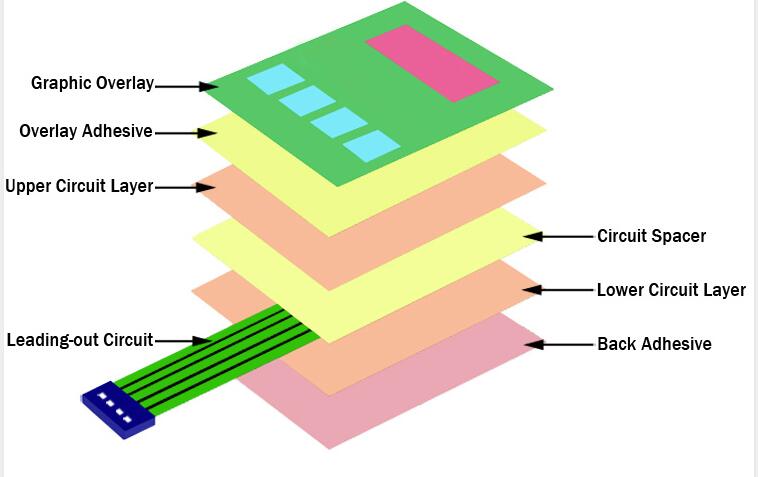
Graphic overlay: no obvious defects (such as lack of strokes in characters that affect readability; stains, light transmission points; deinking, stains, scratches; transparent window overflow, residual glue, etc.); no offset phenomenon (printing Set offset ≤ 0.2mm; combination offset of upper and lower circuit keys ≤ 0.5mm; offset of circuit and key sheet, overlay and key combination ≤ 0.3mm; offset of surrounding blank area after graphic overlay and film circuit combination ≤ 0.2mm ; The offset between the bump and the substrate at the button of the membrane switch panel is ≤0.5mm).
The membrane switch circuit: there must be no residual material scraps, foreign matter, stains, bumps and grease attached to the surface and inside, fingerprints on the circuit, burrs on the edge of the finished product; all circuits and contacts must not have cuts (ie cut marks) Cut from the circuit to the substrate), minor scratches are also based on the principle of not affecting its impedance. The carbon ink surface scratches are based on the principle of not affecting the circuit conduction, and the circuit must not have any foreign matter attached to it.
Conductive silver paste: Generally, the thickness of silver paste is controlled at 7-12μm, and it should be uniform and smooth without obvious defects and pinholes. No disconnection or short circuit is allowed. Carbon ink: The carbon ink covering the silver paste circuit should ensure that the silver paste is completely covered, with a thickness of 8-10μm, and there must be no obvious protrusion of the silver paste.
Insulation printing: no insulating ink is allowed to adhere to all the contact points of the membrane switch. The insulating ink surface should be flat to avoid any defects such as bubbles or pinholes that would affect the insulating effect.
Membrane keypads Bridge circuit: All bridge parts are in accordance with the circuit requirements, and all bridge circuit products must pass 100% open, short circuit and insulation resistance tests. Ensure that there is no open, short circuit and insulation resistance should be greater than 500MΩ (500VDC for 1 minute).
Punching burr and die extrusion switch size: Punching burr and extrusion size should not be greater than plus or minus 0.2mm